Five-layer Co-extruded PEPA Film with Inner Antistatic Layer for Semiconductor
Semiconductor Five-layer PEPA Co-extruded Film with Inner Antistatic Layer
High-purity five-layer PEPA composite film features targeted inner-layer antistatic treatment. It delivers stable ESD protection, ultra-clean contact, superior barrier and mechanical strength, providing dual anti-static and anti-pollution protection for semiconductor precision components.
Our semiconductor-grade five-layer PEPA co-extruded film adopts a professional multi-layer composite structure, combining high-strength PA barrier layers and high-toughness PE sealing layers. The inner contact layer is specially modified with permanent antistatic function, which directly eliminates static accumulation on the packaging contact surface and effectively prevents electrostatic adsorption of dust, micro-particles and fiber debris during component packaging, transportation and storage.
Different from traditional overall blended antistatic film, the targeted inner-layer antistatic design avoids additive migration on the outer surface and maintains ultra-high overall cleanliness. The PA functional layers provide excellent oxygen barrier, puncture resistance and structural stability, while the inner antistatic PE layer ensures safe and clean contact with sensitive semiconductor wafers, chips and precision electronic parts.
Manufactured with high-purity cleanroom-grade raw materials, the film features low particle generation, no silicone contamination and no volatile residues. It perfectly adapts to semiconductor dust-free workshop environments, effectively preventing ESD damage and micro-contamination. The film delivers stable heat-sealing performance and excellent flatness, fully suitable for automatic vacuum packaging and high-standard semiconductor component protection packaging.
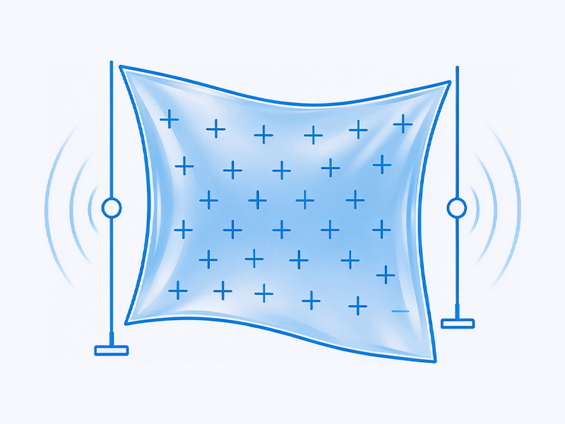
01
Inner-layer Targeted Antistatic Design, Zero Contamination Contact
Antistatic function is concentrated on the inner contact layer only, avoiding full-material additive blending migration. It maintains stable surface resistance, prevents dust adsorption, and ensures ultra-clean contact with precision semiconductor components.
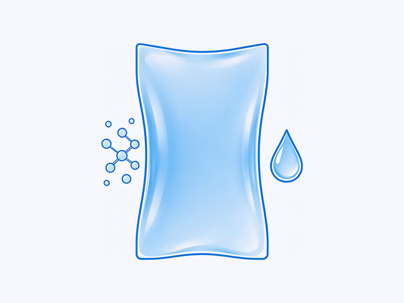
02
PEPA Five-layer Composite, High Barrier & Mechanical Stability
Multi-layer PEPA structure integrates PA high barrier and high toughness with PE excellent heat-sealing performance. It provides outstanding puncture resistance, structural uniformity and oxygen isolation, effectively protecting high-value semiconductor parts.

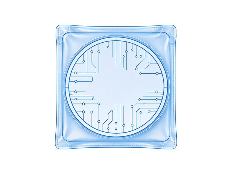
03
Cleanroom Ultra-high Purity, ESD & Particle Double Protection
Produced with semiconductor-grade pure raw materials, low dust generation, no silicone and no residues. The inner antistatic layer eliminates ESD risks while preventing micro-particle contamination, meeting strict semiconductor packaging standards.
| Number of layers | 5 layers |
| Film composition | PE+Antistatic/ PA/ PE+Antistatic |
| Property | Unit of Measure | Value | Procedure |
|---|---|---|---|
| Film thickness | um | 80 | micrometer |
| Tensile strength at break | MPa | 16.79/22.08 | ISO 527-3:2018 |
| Elongation at Break | % | 478.55/635.66 | ISO 527-3:2018 |
| Seal Strength | N/15mm | 45.7 | ASTM F88 |
| Water Vapor Transmission Rate | g/(m2 ·24h) | 4 | ASTM D-1249 |
| Oxygen Transmission Rate | cm3/(m2 ·24h· 0.1 Mpa) | 37.3 | ASTM D-3985 |
| Surface resistivity | Ω | 108-1011 | In-house |