Three-layer Co-extruded Antistatic LDPE Film for Semiconductor Industry
Our three-layer co-extruded antistatic LDPE film is specially developed for high-standard semiconductor precision packaging. Adopting advanced three-layer co-extrusion technology, the film realizes layered functional structure design, separating the antistatic functional layer and the clean contact layer completely. It avoids additive precipitation and ensures ultra-high surface cleanliness.
With stable and lasting antistatic performance, the film effectively eliminates static accumulation and prevents ESD damage to chips, wafers and precision electronic components. The integrated three-layer structure delivers better tensile strength, puncture resistance and overall uniformity compared with conventional single-layer antistatic film.
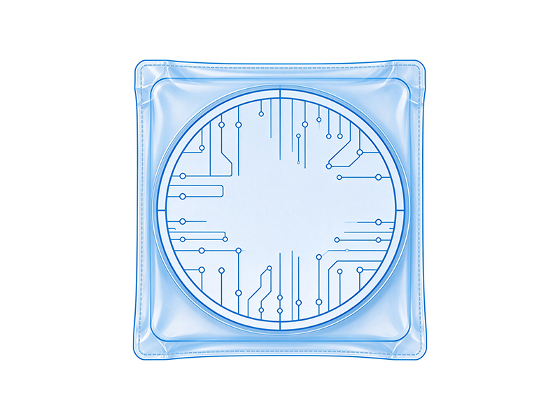
Manufactured from high-purity raw materials with low particle generation, no silicon oil, no impurities and no volatile residues, it fully adapts to Class 100 / Class 1000 cleanroom environments. The film maintains excellent flexibility and stable heat-sealing performance, ensuring smooth automatic packaging, transportation and storage of semiconductor micro-components without dust adsorption or contamination risks.
Cleanroom-grade three-layer co-extruded LDPE film with layered antistatic design achieves zero precipitation and stable ESD protection. Improved mechanical uniformity and ultra-low particle contamination ensure safe and reliable packaging for semiconductor wafers, chips and precision electronic components.
01
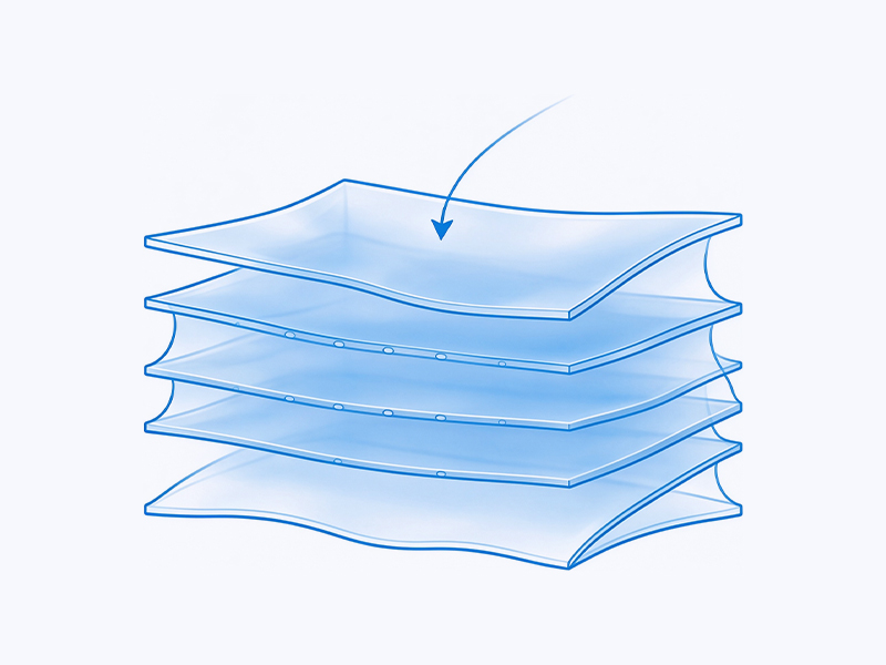
Layered Functional Structure, No Precipitation & Higher Stability
The three-layer co-extruded structure independently arranges the antistatic layer and clean contact layer, preventing antistatic additives from migrating or precipitating. It maintains long-term consistent surface resistance and avoids contaminating precision semiconductor parts.

02
Ultra-clean Cleanroom-grade Purity, Zero Contamination Risk
Produced with high-purity LDPE materials, featuring low dust generation, no silicone, no foreign particles and no volatile residues. It meets strict semiconductor cleanroom packaging standards and protects high-sensitivity wafers and chips from micro-particle pollution.
03
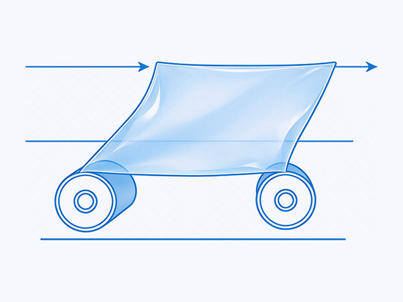
Improved Mechanical Uniformity & Excellent Processing Performance
The composite three-layer structure provides higher film uniformity, better tensile strength and puncture resistance than single-layer film. It performs stably during high-speed automatic bag making and packaging, with no cracking, peeling or particle shedding.
| Number of layers | 3 layers |
| Film composition | PE+Antistatic/ PE/ PE+Antistatic |
| Property | Unit of Measure | Value | Procedure |
|---|---|---|---|
| Film thickness | um | 100 | micrometer |
| Tensile strength at break | MPa | TD30.2 MD36.7 | ISO 527-3:2018 |
| Elongation at Break | % | 1221/1128 | ISO 527-3:2018 |
| Seal Strength | N/15mm | 17.1 | ASTM F88 |
| Water Vapor Transmission Rate | g/(m2 ·24h) | 3.8 | ASTM D-1249 |
| Oxygen Transmission Rate | cm3/(m2 ·24h· 0.1 Mpa) | 1903 | ASTM D-3985 |
| Surface resistivity | Ω | 108-1011 | In-house |